In the world of electronics, the creation of a circuit board is akin to crafting the backbone of technological innovation. Whether you’re a hobbyist diving into DIY projects or an aspiring electronics engineer, understanding the intricacies of making a circuit board is essential. This comprehensive guide will take you through the step-by-step process of crafting your own circuit board, from design to assembly.
Understanding Circuit Board Basics
Before diving into the pcb manufacturing process, it’s crucial to grasp the fundamental components of a circuit board. Learn about the different layers, such as the substrate, copper traces, solder mask, and silkscreen, and how each contributes to the functionality and aesthetics of the board.
What is a circuit board?
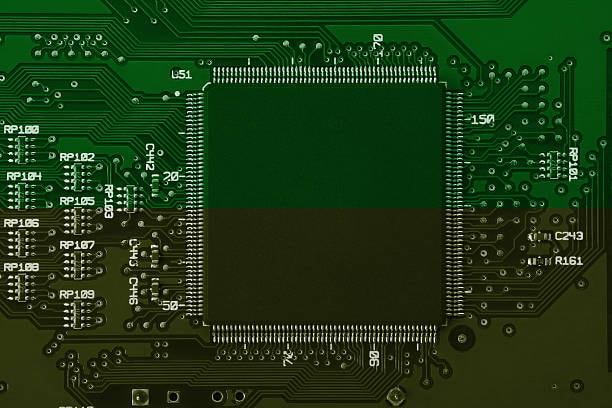
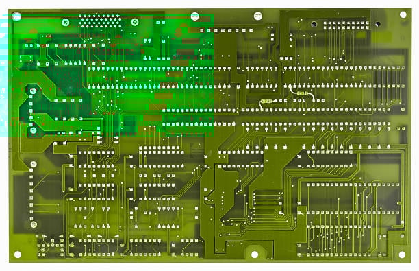
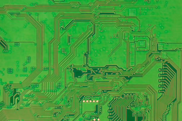
A circuit board, also known as a printed circuit board (PCB), is a flat, rigid board made of insulating material with thin layers of copper foil etched onto its surface. These copper traces act as pathways for electrical signals to flow between electronic components like resistors, capacitors, and integrated circuits (ICs) that are mounted on the board. The board’s design and layout, created using specialized software, determine how these components are interconnected to form functional circuits. Circuit boards are essential in electronic devices, providing a stable platform for components and enabling the creation of complex electrical systems in a compact and organized manner.
What are the different ways to make a Circuit Board?
There are several methods for making circuit boards, each with its advantages and applications:
Etching Method

In this traditional method, a copper-clad substrate is coated with a resist material. A circuit pattern is then transferred onto the resist using a template or photochemical process. The exposed copper is etched away using an acid solution, leaving behind the desired copper traces. This method is suitable for prototyping and small-scale production but may require specialized equipment and handling of hazardous chemicals.
Milling Method

The milling method involves using a CNC (Computer Numerical Control) machine to remove copper from a substrate according to a digital design file. The machine precisely mills away excess copper to create the desired circuit traces and features. This method offers high accuracy and is suitable for producing complex PCBs with fine details. However, it may be slower than other methods and requires a CNC machine.
Printing Method
In the printing method, conductive ink or paste is printed onto a substrate using inkjet, screen printing, or stencil printing techniques. The ink forms the circuit traces, and additional layers such as solder mask and silkscreen may be applied using similar printing processes. This method is fast and cost-effective for producing prototypes and low-volume boards but may have limitations in terms of resolution and durability.
DIY Methods
DIY enthusiasts and hobbyists often use methods like toner transfer or direct copper deposition to create circuit boards at home. Toner transfer involves printing the circuit pattern onto special transfer paper using a laser printer and then transferring the toner onto a copper-clad board through heat and pressure. Direct copper deposition uses conductive ink or paint to draw circuit traces directly onto the substrate. While these methods are accessible and affordable for small projects, they may not offer the same precision and reliability as professional fabrication methods.
Prototyping Services
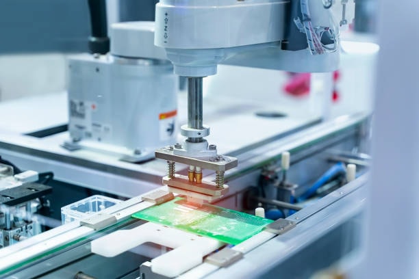
Many companies offer prototyping services where users can upload their circuit designs, and the company fabricates the boards using advanced manufacturing techniques like photo lithography and chemical etching. These services provide high-quality PCBs with quick turnaround times, making them ideal for prototyping and small-batch production.
What Materials are Required to Make a Circuit Board?
To make a circuit board, you’ll need several materials, each playing a crucial role in the fabrication process:
Substrate Material
The substrate is the base material of the PCB, providing mechanical support and insulation between copper traces. Common substrate materials include fiberglass (FR-4), phenolic paper, and polyimide (flexible PCBs). Choose a substrate material based on the application’s requirements, such as rigidity, flexibility, and thermal properties.
Copper Clad Board
A copper-clad board consists of a substrate material coated with a thin layer of copper foil. The copper serves as the conductive pathways (traces) for electrical signals between components. Copper thickness varies depending on the application’s current-carrying capacity and impedance requirements.
Etching Chemicals
If using the etching method, you’ll need etching chemicals such as ferric chloride or ammonium persulfate. These chemicals remove unwanted copper from the board, leaving behind the desired circuit traces. Follow safety guidelines when handling etching chemicals, as they can be corrosive and hazardous.
Resist Material
Resist material is used to protect areas of the copper-clad board from etching. Photoresist is commonly used in photolithography processes, where UV light exposes the resist to create the circuit pattern. Dry film resist or solder mask can also be applied to the board’s surface to protect areas during etching or soldering.
Solder and Flux
Solder is used to attach components to the circuit board and create electrical connections. Choose solder with appropriate alloy composition (e.g., lead-free solder for environmental compliance). Flux is applied to the solder joints to improve wetting and remove oxidation, ensuring reliable solder connections.
Components
Electronic components include resistors, capacitors, diodes, transistors, integrated circuits (ICs), connectors, and more. Select components based on the circuit design and desired functionality. Components are soldered onto the board during assembly.
Silkscreen Ink
Silkscreen ink is used to apply component markings, labels, logos, and reference indicators onto the circuit board. It helps identify components and their placement, enhancing the board’s usability and aesthetics.
Protective Coatings
Protective coatings like solder mask and conformal coating are applied to the board’s surface for insulation, corrosion resistance, and environmental protection. Solder mask covers exposed copper traces to prevent short circuits, while conformal coating shields components from moisture, dust, and chemical exposure.
How to make a circuit board?

Sure, here’s a short paragraph for each step of making a circuit board:
Designing the Circuit
Start by designing your circuit using PCB design software. Place components, route traces, and optimize the layout for efficiency and functionality.
Printing the Layout
Print the circuit layout onto special transfer paper using a laser printer. Ensure the design is mirrored and scaled correctly.
Transferring the Design
Place the printed layout onto a copper-clad board and apply heat and pressure using a laminator or iron. This transfers the toner onto the board.
Etching the Board
Submerge the board in an etching solution such as ferric chloride or ammonium persulfate. The solution removes excess copper, leaving behind the circuit traces.
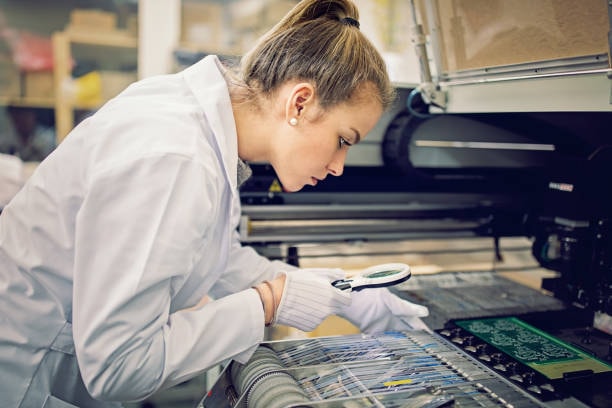
Cleaning and Inspecting
After etching, clean the board thoroughly to remove any remaining toner and etching residue. Inspect the board for any defects or incomplete traces.
Drilling Holes
Use a drill with a fine bit to drill holes for component placement and soldering. Ensure the hole sizes match your component leads.
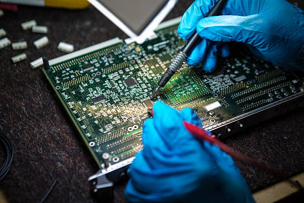
Soldering Components
Place electronic components onto the board and solder them to the circuit traces. Follow proper soldering techniques to create secure and reliable connections.
Applying Protective Coatings
Apply solder mask to cover exposed copper traces and prevent short circuits. Optionally, apply a conformal coating for additional protection against environmental factors.
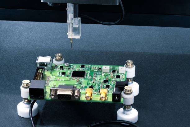
Testing and Troubleshooting
Test the completed circuit board for functionality and performance. Use multimeters, oscilloscopes, and other testing tools to identify and troubleshoot any issues.
Finalizing the Board
Label components using silkscreen ink for identification. Verify that the board meets design specifications and standards before final assembly and integration into your electronic device.
Conclusion
In conclusion, mastering the art of making a circuit board is a rewarding journey that blends technical skills with creativity and precision. By following the comprehensive guide outlined here, you have gained insights into the step-by-step process of designing, fabricating, and assembling a functional PCB. From understanding circuit board basics to applying protective coatings and testing for functionality, each stage contributes to the creation of a reliable and efficient electronic component.
As you continue to explore the world of electronics and PCB design, remember that practice and experimentation are key to refining your skills. Embrace challenges, learn from mistakes, and leverage resources such as PCB design software, fabrication tools, and testing equipment to enhance your proficiency. Whether you’re a hobbyist working on DIY projects or a professional engineer developing cutting-edge technology, the knowledge and techniques gained from this guide will empower you to create innovative and impactful electronic devices with confidence.
Summary
In this comprehensive guide, we’ve delved into the intricate process of making a circuit board, from conceptualizing the design to the final assembly. We began by understanding the fundamental components of a circuit board, including the substrate, copper traces, solder mask, and silkscreen. Through detailed explanations, we explored various methods of fabricating circuit boards, such as etching, milling, printing, and DIY approaches, each offering unique benefits and applications.
Moving forward, we discussed the essential materials required for making a circuit board, including substrate materials, copper-clad boards, etching chemicals, resist materials, solder, components, silkscreen ink, and protective coatings. By highlighting the step-by-step process of designing the circuit, transferring the design onto the board, etching, drilling, soldering components, applying protective coatings, and testing for functionality, this guide provides a comprehensive roadmap for anyone looking to master the art of creating electronic circuits. Whether you’re a beginner exploring PCB fabrication or an experienced engineer seeking to refine your techniques, the insights and techniques shared here empower you to embark on your circuit board creation journey with confidence and expertise.